Our Standard Flip Chip process, formerly known as the Flex-on-Cap (or FoC) process, was originally developed in the mid-1960’s by Delco for use in the automotive industry. Today, the process has unsurpassed industry track record with 40 years and millions of bumped wafers behind it. This is the process to use when you need to place small bumps (less than 130μm in height) directly on the die I/O.

Typically, the number of bumps per die ranges from 4 to 6000. The Standard FlipChip process uses premixed solder paste for the solder bumps. This provides for outstanding control of the alloy composition across the entire wafer. Since the process is not limited to the bi-metal constraints of an electroplating process, a wide range of multi-metal solder alloys tailored to your application (such as Sn/Ag/Cu alloys) are available. As with all flip chip die processed with small bumps, these die will require the use of underfilling during packaging in order to achieve acceptable reliability.

/
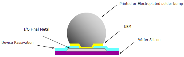
Bump on I/O Flip chip

Our Standard FlipChip-Repassivation process flows are similar to the Standard FlipChip-Bump on I/O process, but support bumping applications that do not meet all of the I/O final metal pad and passivation opening requirements of Standard FlipChip-Bump on I/O. In this process, a stress relieving layer of either Benzocyclobutene (BCB) or Polybenzoxazoles (PBO) is deposited on the die before bumping. The repassivation layer corrects for the issue of the I/O passivation opening being too small or too large for a standard flip chip bump. It also corrects for the issue of the I/O final metal pad being too small for a standard flip chip bump. The repassivation dielectric layer also planarizes the device surface and gives the bump structure additional strength and robustness.

/
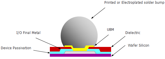
Repassivated Flip chip
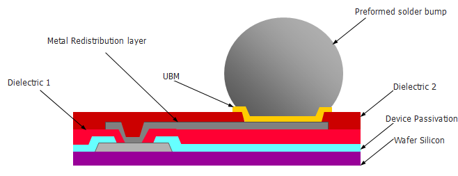
On some die, the I/O are not located where you need to have the bumps. This is especially true when you take a die originally designed for wire bond packaging applications and need to convert it to be flip chip compatible. The Standard FlipChip-Redistribution Line (or RDL) process adds “redistribution metallization” (often called “runners’ or “traces”) that let you re-route the signal path from the die peripheral I/O to an area array of new bump locations, often with significant loosening of effective bump pitches.

/
RDL Flip chip

In this flip chip bumping alternative, a dielectric repassivation layer of either Benzocyclobutene (or BCB) or Polybenzoxazoles (PBO) can be selected as a localized stress reliever in the bump location on the die before bumping. As with Standard FlipChip-Bump on I/O and Standard FlipChip-Repassivation, FCI’s Cu Pillar Bump – Repassivation offering is designed for small flip chip bumping applications (less than 130μm in diameter) placed directly on the die I/O. FCI’s Cu Pillar Bump can also be readily incorporated with FCI’s plated Cu RDL options should it be required.

/
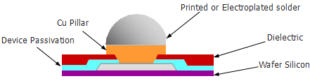
Repassivated Cu Pillar